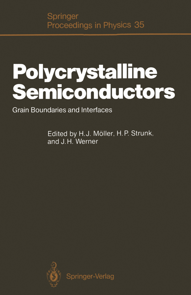
Polycrystalline Semiconductors
Grain Boundaries and Interfaces
Polycrystalline Semiconductors
Grain Boundaries and Interfaces
This book contains the papers presented at the international symposium Polycrys talline Semiconductors - Grain Boundaries and Interfaces (POLYSE '88) that was held in Malente, FRG, from August 29 to September 2, 1988. This conference has two roots: Firstly, it is a successor to a conference on polycrystalline semi conductors held in Perpignan, France, in 1982 and to a summer school in Erice, Italy, in 1984. Secondly, it continues a series of German workshops on polycrys talline semiconductors, which have been organized every year since 1983 by two of the present editors (H. P. S. and J. H. W. ) in Stuttgart, FRG. As in these previ ous workshops, the symposium POLYSE '88 also tried to bridge the gap between fundamental research and technological aspects of polycrystalline semiconductors with emphasis on physical properties. In order to realize this conception, 12 scientists recognized in their fields were invited to give reviews of their respective work. The expert presentations of these scientists complemented by all other contributions, including an ad hoc evening workshop on the chemical analysis of grain boundaries by scanning tunneling microscopy, resulted in a lively and rewarding symposium. We would particularly like to thank the invited speakers for their talks, as well as for undertaking the task of refereeing the submitted papers. These speakers are: L. N. Aleksandrov Y. Ishida P. Pirouz A. Bourret J. D. Joannopoulos H. W. Schock H. Cerva L. L. Kazmerski H. Teichler F. Greuter S. Martinuzzi K. N.
Grain Boundary Structure Determination by HREM: A Comparison with Computer Relaxed Configurations for Pure Tilt in Germanium
Multiple Structures of a [001] ? = 13 Tilt Grain Boundary in Germanium
Computer Modelling of Grain Boundaries by Use of Interatomic Potentials
Transmission of Dislocations with Non-common Burgers Vectors Through ? = 9 (12?2) Boundaries in Silicon and Germanium Observed by In Situ HVEM
II Grain Boundary Chemistry and Electronic Properties
High Resolution Electron Microscopy of the Structure and Chemistry of Grain Boundaries and Other Interfaces in Semiconductors
Theoretical Studies of the Impurity Segregation and Electrical Properties of Polycrystalline Silicon by LCAO Electronic Theory
Electronic Properties of ? = 25 Silicon Bicrystals by Deep Level Transient Spectroscopy
The Influence of Structure and Impurity Precipitation on the Electrical Properties of the Grain Boundaries in Silicon: Copper Precipitation in the ? = 25 Boundary
EBIC Contrast and Precipitation in ? = 13 and ? = 25 Annealed Silicon Bicrystals
Electron Beam Induced Current Contrast and Transmission Electron Microscopy Analysis of Special Grain Boundaries in Silicon
SEM-EBIC Investigations of the Electrical Activity of Grain Boundaries in Germanium
III Segregation, Activation and Passivation
Atomic-Level Imaging and Microanalysis of Grain Boundaries in Polycrystalline Semiconductors
Investigation of the Cobalt Segregation at Grain Boundaries in Silicon
On the Influence of the Cottrell Atmosphere on the Recombination Losses at Grain Boundaries in Polycrystalline Silicon
Hydrogen Passivation of Grain Boundaries in Silicon Sheet Material.-Atomic Hydrogen Passivation Studies of Microcrystalline Phases in Ion-Implant Damaged Surface Layers of Silicon
Hydrogen Injection and Migration in Silicon
Analysis of the Polycrystalline Semiconducting Film Electrical Resistance Variation Due to Isothermal Desorption and Temperature Stimulated Desorption of Oxygen
IV Segregation, Activation and Passivation
Activation and Passivation of Grain Boundary Recombination Activity in Polycrystalline Silicon
Thermal Activation and Hydrogen Passivation of Grain Boundaries
Analysis of Metal-Doped Polycrystalline Silicon with Secondary Ion Mass Spectrometry
Oxygen Detection in Polycrystalline Silicon
Generation of Radiation Defects in the Vicinity of Twin Boundaries in EFG Silicon Ribbons
Physical Properties of Polycrystalline S-Web Si Ribbons
Grain Boundary Structure in S-WEB Silicon Ribbon
Characterization of MBE-Grown Polysilicon
V Technology
Mechanisms of Epitaxial Growth of Polar Semiconductors on (001) Silicon
Preparation and Characterization of Nickel Silicide
Characterization of the Interface of Silicon pn-Junctions, Fabricated by the Silicon Direct Bonding (SDB) Method
Metal and Polycrystalline Silicon Reactions
Interfacial Reactions of TiNx/Si Contacts
Linear and Parabolic Growth Kinetics in Binary Couples
VI Thin Films
Polycrystalline Compound Semiconductor Thin Films in Solar Cells
Electronic Properties of Photoetched CdSe Films
Thin Film Transistors and Light Sensors with Polycrystalline CdSe-Semiconductors
VII Crystallization
Crystallization Processes and Structures of Semiconductor Films
Crystallized Silicon Films for Active Devices
Laser Recrystallization of Polysilicon for Improved Device Quality
Growth of Sb-Doped Epitaxial Si Layers Through Recrystallizationof Poly-Si on a (100) Si Substrate
VIII Transport Properties
Current Control by Electrically Active Grain Boundaries
Numerical Modelling of the Intergranular Potential Barrier Height and Carrier Concentration in Polysilicon
Hall Mobility and Carrier Concentration of e-Gun Evaporated Poly-Si Films
Measurement and Calculation of the Carrier Concentration in Polycrystalline Germanium Thin Films
Grain Boundary States in Float-Zone Silicon Bicrystals
Pressure Studies of Metastable Electron Traps in Grain Boundaries of p-HgMnTe and p-HgCdMnTe
Band Tailing in Polycrystalline and Disordered Silicon
IX Thin Films
Microstructure and Interfaces of Polysilicon in Integrated Circuits
Effect of the Grain Boundaries in Small Grain Polysilicon Thin Film Transistors
Kink Effect in the Double-Gate Accumulation-Mode N-Channel Polysilicon Thin-Film Transistors
Applications of Poly-Si in Selective-Area and Three-Dimensional Devices
Thin-Film Transistors from Evaporated Low Temperature Processed Poly-Si Films
Pressure Effect on In Situ Boron-Doped LPCVD Silicon Films
Index of Contributors.
I Grain Boundary Structure
Intergranular Total Energy Maps and the Structure of a Grain BoundaryGrain Boundary Structure Determination by HREM: A Comparison with Computer Relaxed Configurations for Pure Tilt in Germanium
Multiple Structures of a [001] ? = 13 Tilt Grain Boundary in Germanium
Computer Modelling of Grain Boundaries by Use of Interatomic Potentials
Transmission of Dislocations with Non-common Burgers Vectors Through ? = 9 (12?2) Boundaries in Silicon and Germanium Observed by In Situ HVEM
II Grain Boundary Chemistry and Electronic Properties
High Resolution Electron Microscopy of the Structure and Chemistry of Grain Boundaries and Other Interfaces in Semiconductors
Theoretical Studies of the Impurity Segregation and Electrical Properties of Polycrystalline Silicon by LCAO Electronic Theory
Electronic Properties of ? = 25 Silicon Bicrystals by Deep Level Transient Spectroscopy
The Influence of Structure and Impurity Precipitation on the Electrical Properties of the Grain Boundaries in Silicon: Copper Precipitation in the ? = 25 Boundary
EBIC Contrast and Precipitation in ? = 13 and ? = 25 Annealed Silicon Bicrystals
Electron Beam Induced Current Contrast and Transmission Electron Microscopy Analysis of Special Grain Boundaries in Silicon
SEM-EBIC Investigations of the Electrical Activity of Grain Boundaries in Germanium
III Segregation, Activation and Passivation
Atomic-Level Imaging and Microanalysis of Grain Boundaries in Polycrystalline Semiconductors
Investigation of the Cobalt Segregation at Grain Boundaries in Silicon
On the Influence of the Cottrell Atmosphere on the Recombination Losses at Grain Boundaries in Polycrystalline Silicon
Hydrogen Passivation of Grain Boundaries in Silicon Sheet Material.-Atomic Hydrogen Passivation Studies of Microcrystalline Phases in Ion-Implant Damaged Surface Layers of Silicon
Hydrogen Injection and Migration in Silicon
Analysis of the Polycrystalline Semiconducting Film Electrical Resistance Variation Due to Isothermal Desorption and Temperature Stimulated Desorption of Oxygen
IV Segregation, Activation and Passivation
Activation and Passivation of Grain Boundary Recombination Activity in Polycrystalline Silicon
Thermal Activation and Hydrogen Passivation of Grain Boundaries
Analysis of Metal-Doped Polycrystalline Silicon with Secondary Ion Mass Spectrometry
Oxygen Detection in Polycrystalline Silicon
Generation of Radiation Defects in the Vicinity of Twin Boundaries in EFG Silicon Ribbons
Physical Properties of Polycrystalline S-Web Si Ribbons
Grain Boundary Structure in S-WEB Silicon Ribbon
Characterization of MBE-Grown Polysilicon
V Technology
Mechanisms of Epitaxial Growth of Polar Semiconductors on (001) Silicon
Preparation and Characterization of Nickel Silicide
Characterization of the Interface of Silicon pn-Junctions, Fabricated by the Silicon Direct Bonding (SDB) Method
Metal and Polycrystalline Silicon Reactions
Interfacial Reactions of TiNx/Si Contacts
Linear and Parabolic Growth Kinetics in Binary Couples
VI Thin Films
Polycrystalline Compound Semiconductor Thin Films in Solar Cells
Electronic Properties of Photoetched CdSe Films
Thin Film Transistors and Light Sensors with Polycrystalline CdSe-Semiconductors
VII Crystallization
Crystallization Processes and Structures of Semiconductor Films
Crystallized Silicon Films for Active Devices
Laser Recrystallization of Polysilicon for Improved Device Quality
Growth of Sb-Doped Epitaxial Si Layers Through Recrystallizationof Poly-Si on a (100) Si Substrate
VIII Transport Properties
Current Control by Electrically Active Grain Boundaries
Numerical Modelling of the Intergranular Potential Barrier Height and Carrier Concentration in Polysilicon
Hall Mobility and Carrier Concentration of e-Gun Evaporated Poly-Si Films
Measurement and Calculation of the Carrier Concentration in Polycrystalline Germanium Thin Films
Grain Boundary States in Float-Zone Silicon Bicrystals
Pressure Studies of Metastable Electron Traps in Grain Boundaries of p-HgMnTe and p-HgCdMnTe
Band Tailing in Polycrystalline and Disordered Silicon
IX Thin Films
Microstructure and Interfaces of Polysilicon in Integrated Circuits
Effect of the Grain Boundaries in Small Grain Polysilicon Thin Film Transistors
Kink Effect in the Double-Gate Accumulation-Mode N-Channel Polysilicon Thin-Film Transistors
Applications of Poly-Si in Selective-Area and Three-Dimensional Devices
Thin-Film Transistors from Evaporated Low Temperature Processed Poly-Si Films
Pressure Effect on In Situ Boron-Doped LPCVD Silicon Films
Index of Contributors.
Möller, Hans J.
Strunk, Horst P.
Werner, Juergen
| ISBN | 978-3-642-93415-5 |
|---|---|
| Medientyp | Buch |
| Copyrightjahr | 2014 |
| Verlag | Springer, Berlin |
| Umfang | XI, 394 Seiten |
| Sprache | Englisch |

